Event submissions
Published

This submission belongs to the session IAP. Industry Application posters of the event Holography Meets Advanced Manufacturing
Published date
13 Mar, 2023
Academic Editor
'%3e%3cpath%20d='M12.6657%2010.9104C12.4185%2010.325%2012.0599%209.79327%2011.6097%209.34482C11.1609%208.89508%2010.6293%208.5365%2010.0442%208.28888C10.0389%208.28626%2010.0337%208.28495%2010.0285%208.28233C10.8446%207.69279%2011.3752%206.73249%2011.3752%205.64904C11.3752%203.8542%209.92103%202.39999%208.1262%202.39999C6.33136%202.39999%204.87715%203.8542%204.87715%205.64904C4.87715%206.73249%205.40774%207.69279%206.22393%208.28364C6.21869%208.28626%206.21345%208.28757%206.20821%208.29019C5.62129%208.5378%205.09463%208.89284%204.64265%209.34613C4.1929%209.79493%203.83432%2010.3266%203.58671%2010.9117C3.34345%2011.4845%203.21226%2012.0987%203.20023%2012.7209C3.19988%2012.7349%203.20233%2012.7488%203.20744%2012.7619C3.21255%2012.7749%203.22022%2012.7867%203.22998%2012.7968C3.23975%2012.8068%203.25142%2012.8147%203.26431%2012.8202C3.2772%2012.8256%203.29105%2012.8284%203.30504%2012.8284H4.09109C4.14874%2012.8284%204.19459%2012.7825%204.1959%2012.7262C4.2221%2011.7148%204.62823%2010.7676%205.34617%2010.0497C6.08899%209.30683%207.0755%208.89808%208.1262%208.89808C9.17689%208.89808%2010.1634%209.30683%2010.9062%2010.0497C11.6242%2010.7676%2012.0303%2011.7148%2012.0565%2012.7262C12.0578%2012.7838%2012.1037%2012.8284%2012.1613%2012.8284H12.9474C12.9613%2012.8284%2012.9752%2012.8256%2012.9881%2012.8202C13.001%2012.8147%2013.0126%2012.8068%2013.0224%2012.7968C13.0322%2012.7867%2013.0398%2012.7749%2013.0449%2012.7619C13.0501%2012.7488%2013.0525%2012.7349%2013.0522%2012.7209C13.0391%2012.0947%2012.9094%2011.4855%2012.6657%2010.9104ZM8.1262%207.9024C7.52486%207.9024%206.9589%207.6679%206.53312%207.24211C6.10733%206.81633%205.87283%206.25037%205.87283%205.64904C5.87283%205.0477%206.10733%204.48174%206.53312%204.05596C6.9589%203.63018%207.52486%203.39567%208.1262%203.39567C8.72753%203.39567%209.29349%203.63018%209.71927%204.05596C10.1451%204.48174%2010.3796%205.0477%2010.3796%205.64904C10.3796%206.25037%2010.1451%206.81633%209.71927%207.24211C9.29349%207.6679%208.72753%207.9024%208.1262%207.9024Z'%20fill='%235D1EE1'/%3e%3c/g%3e%3c/svg%3e) VIJAYAKUMAR ANAND
VIJAYAKUMAR ANANDCitation
Pranuti Pamula, Aravindhan Alagarsamy, Durga Prasad Gorthy, Phalguni Singh Ngangbam, Verification of SoC using Advanced Verification Methodology, in Proceedings of Holography Meets Advanced Manufacturing, 20 February–22 February 2023, MDPI: Basel, Switzerland, doi: 10.3390/HMAM2-14160
Share
Email
Facebook
Twitter
LinkedIn
Verification of SoC using Advanced Verification Methodology
'%3e%3cpath%20d='M12.6647%2010.9104C12.4176%2010.325%2012.0589%209.7933%2011.6088%209.34485C11.16%208.89511%2010.6283%208.53653%2010.0432%208.28891C10.038%208.28629%2010.0327%208.28498%2010.0275%208.28236C10.8437%207.69282%2011.3743%206.73252%2011.3743%205.64907C11.3743%203.85423%209.92005%202.40002%208.12522%202.40002C6.33038%202.40002%204.87618%203.85423%204.87618%205.64907C4.87618%206.73252%205.40677%207.69282%206.22296%208.28367C6.21772%208.28629%206.21248%208.2876%206.20724%208.29022C5.62031%208.53783%205.09365%208.89287%204.64167%209.34616C4.19192%209.79496%203.83334%2010.3266%203.58573%2010.9117C3.34247%2011.4846%203.21128%2012.0987%203.19925%2012.721C3.1989%2012.735%203.20135%2012.7489%203.20646%2012.7619C3.21157%2012.7749%203.21924%2012.7868%203.22901%2012.7968C3.23877%2012.8068%203.25045%2012.8148%203.26334%2012.8202C3.27623%2012.8256%203.29007%2012.8284%203.30406%2012.8284H4.09012C4.14776%2012.8284%204.19362%2012.7825%204.19493%2012.7262C4.22113%2011.7148%204.62726%2010.7676%205.34519%2010.0497C6.08802%209.30686%207.07452%208.89811%208.12522%208.89811C9.17592%208.89811%2010.1624%209.30686%2010.9052%2010.0497C11.6232%2010.7676%2012.0293%2011.7148%2012.0555%2012.7262C12.0568%2012.7839%2012.1027%2012.8284%2012.1603%2012.8284H12.9464C12.9604%2012.8284%2012.9742%2012.8256%2012.9871%2012.8202C13%2012.8148%2013.0117%2012.8068%2013.0214%2012.7968C13.0312%2012.7868%2013.0389%2012.7749%2013.044%2012.7619C13.0491%2012.7489%2013.0515%2012.735%2013.0512%2012.721C13.0381%2012.0947%2012.9084%2011.4856%2012.6647%2010.9104ZM8.12522%207.90243C7.52388%207.90243%206.95792%207.66793%206.53214%207.24215C6.10636%206.81636%205.87185%206.2504%205.87185%205.64907C5.87185%205.04773%206.10636%204.48177%206.53214%204.05599C6.95792%203.63021%207.52388%203.3957%208.12522%203.3957C8.72655%203.3957%209.29252%203.63021%209.7183%204.05599C10.1441%204.48177%2010.3786%205.04773%2010.3786%205.64907C10.3786%206.2504%2010.1441%206.81636%209.7183%207.24215C9.29252%207.66793%208.72655%207.90243%208.12522%207.90243Z'%20fill='%235D1EE1'/%3e%3c/g%3e%3c/svg%3e)
Pranuti Pamula 1
Aravindhan Alagarsamy 1
Durga Prasad Gorthy 2
Phalguni Singh Ngangbam 1
1. Multi-Core Architecture Computation (MAC) Lab, Department of Electronics and
Communication Engineering, Koneru Lakshmaiah Education Foundation, India
2. SMTS Silicon Design Engineer
AMD,Hyderabad
Telangana,India
Abstract
The semiconductor industry has evolved significantly since its founding in the 1950. Primarily used electronic devices like transistors and diodes, but advancements in technology have led to more complex and powerful semiconductor devices , from printed circuit boards to a multi-million gate design i.e. a System on Chip. SoC provides faster and reliable implementation design with low cost per gate and considerably low power consumption. In addition , it offers a smaller physical size and with greater design security. Almost 70-80 percent of the total SoC design effort is spent on the functional verification. For meeting requirement the traditional simulation methods are no longer sufficient for the system level verification. This kind of verification platform which supports a mixed functional verification with both IP core level and system level. In this thesis, verification of interconnect block in a processing system is presented. The functional verification of the design is done by using system verilog and UVM . The verification process includes creation of testcases, assertions and checkers for verifying different functionality as per the design specifications. The connectivity of the interconnect to the masters and the corresponding slaves is verified by memory mapped registers. A unique functional block which is present on the interconnect to slave interface is verified by using combination of checkers and test sequences. Performance and trace monitoring of the transactions on AXI interface of the interconnect is done by programming different operational pointers and filters. Simulated results from the Synopsys - VCS tool verifies functional correctness of the design.
Keywords
semiconductor indusry
SoC
functional verification
System Verilog
UVM
AXI interface
Manuscript
Project Paper Final (1).pdf
Poster
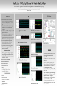
poster presentation (1) (1).pdf
Design and simulation of a low power and high speed Fast Fourier Transform for medical image compression
IMPLEMENTATION OF CONTENT-BASED IMAGE RETRIEVAL USING ARTIFICIAL NEURAL NETWORKS