Event submissions
Published
This submission belongs to the session D. Electrical, Electronics and Communications Engineering of the event The 4th International Electronic Conference on Applied Sciences
Published date
27 Oct, 2023
Academic Editor
'%3e%3cpath%20d='M12.6657%2010.9104C12.4185%2010.325%2012.0599%209.79327%2011.6097%209.34482C11.1609%208.89508%2010.6293%208.5365%2010.0442%208.28888C10.0389%208.28626%2010.0337%208.28495%2010.0285%208.28233C10.8446%207.69279%2011.3752%206.73249%2011.3752%205.64904C11.3752%203.8542%209.92103%202.39999%208.1262%202.39999C6.33136%202.39999%204.87715%203.8542%204.87715%205.64904C4.87715%206.73249%205.40774%207.69279%206.22393%208.28364C6.21869%208.28626%206.21345%208.28757%206.20821%208.29019C5.62129%208.5378%205.09463%208.89284%204.64265%209.34613C4.1929%209.79493%203.83432%2010.3266%203.58671%2010.9117C3.34345%2011.4845%203.21226%2012.0987%203.20023%2012.7209C3.19988%2012.7349%203.20233%2012.7488%203.20744%2012.7619C3.21255%2012.7749%203.22022%2012.7867%203.22998%2012.7968C3.23975%2012.8068%203.25142%2012.8147%203.26431%2012.8202C3.2772%2012.8256%203.29105%2012.8284%203.30504%2012.8284H4.09109C4.14874%2012.8284%204.19459%2012.7825%204.1959%2012.7262C4.2221%2011.7148%204.62823%2010.7676%205.34617%2010.0497C6.08899%209.30683%207.0755%208.89808%208.1262%208.89808C9.17689%208.89808%2010.1634%209.30683%2010.9062%2010.0497C11.6242%2010.7676%2012.0303%2011.7148%2012.0565%2012.7262C12.0578%2012.7838%2012.1037%2012.8284%2012.1613%2012.8284H12.9474C12.9613%2012.8284%2012.9752%2012.8256%2012.9881%2012.8202C13.001%2012.8147%2013.0126%2012.8068%2013.0224%2012.7968C13.0322%2012.7867%2013.0398%2012.7749%2013.0449%2012.7619C13.0501%2012.7488%2013.0525%2012.7349%2013.0522%2012.7209C13.0391%2012.0947%2012.9094%2011.4855%2012.6657%2010.9104ZM8.1262%207.9024C7.52486%207.9024%206.9589%207.6679%206.53312%207.24211C6.10733%206.81633%205.87283%206.25037%205.87283%205.64904C5.87283%205.0477%206.10733%204.48174%206.53312%204.05596C6.9589%203.63018%207.52486%203.39567%208.1262%203.39567C8.72753%203.39567%209.29349%203.63018%209.71927%204.05596C10.1451%204.48174%2010.3796%205.0477%2010.3796%205.64904C10.3796%206.25037%2010.1451%206.81633%209.71927%207.24211C9.29349%207.6679%208.72753%207.9024%208.1262%207.9024Z'%20fill='%235D1EE1'/%3e%3c/g%3e%3c/svg%3e) Andrea Ballo
Andrea BalloCitation
Enrico Brugnolotto, Claudia Mezzalira, Fosca Conti, Danilo Pedron, Raffaella Signorini, 2D Micro-Raman mapping of thermomechanical local stress in assembled GaN LEDs and Si chips , in Proceedings of The 4th International Electronic Conference on Applied Sciences, 27 October–10 November 2023, MDPI: Basel, Switzerland
Share
Email
Facebook
Twitter
LinkedIn
2D Micro-Raman mapping of thermomechanical local stress in assembled GaN LEDs and Si chips
'%3e%3cpath%20d='M12.6647%2010.9104C12.4176%2010.325%2012.0589%209.7933%2011.6088%209.34485C11.16%208.89511%2010.6283%208.53653%2010.0432%208.28891C10.038%208.28629%2010.0327%208.28498%2010.0275%208.28236C10.8437%207.69282%2011.3743%206.73252%2011.3743%205.64907C11.3743%203.85423%209.92005%202.40002%208.12522%202.40002C6.33038%202.40002%204.87618%203.85423%204.87618%205.64907C4.87618%206.73252%205.40677%207.69282%206.22296%208.28367C6.21772%208.28629%206.21248%208.2876%206.20724%208.29022C5.62031%208.53783%205.09365%208.89287%204.64167%209.34616C4.19192%209.79496%203.83334%2010.3266%203.58573%2010.9117C3.34247%2011.4846%203.21128%2012.0987%203.19925%2012.721C3.1989%2012.735%203.20135%2012.7489%203.20646%2012.7619C3.21157%2012.7749%203.21924%2012.7868%203.22901%2012.7968C3.23877%2012.8068%203.25045%2012.8148%203.26334%2012.8202C3.27623%2012.8256%203.29007%2012.8284%203.30406%2012.8284H4.09012C4.14776%2012.8284%204.19362%2012.7825%204.19493%2012.7262C4.22113%2011.7148%204.62726%2010.7676%205.34519%2010.0497C6.08802%209.30686%207.07452%208.89811%208.12522%208.89811C9.17592%208.89811%2010.1624%209.30686%2010.9052%2010.0497C11.6232%2010.7676%2012.0293%2011.7148%2012.0555%2012.7262C12.0568%2012.7839%2012.1027%2012.8284%2012.1603%2012.8284H12.9464C12.9604%2012.8284%2012.9742%2012.8256%2012.9871%2012.8202C13%2012.8148%2013.0117%2012.8068%2013.0214%2012.7968C13.0312%2012.7868%2013.0389%2012.7749%2013.044%2012.7619C13.0491%2012.7489%2013.0515%2012.735%2013.0512%2012.721C13.0381%2012.0947%2012.9084%2011.4856%2012.6647%2010.9104ZM8.12522%207.90243C7.52388%207.90243%206.95792%207.66793%206.53214%207.24215C6.10636%206.81636%205.87185%206.2504%205.87185%205.64907C5.87185%205.04773%206.10636%204.48177%206.53214%204.05599C6.95792%203.63021%207.52388%203.3957%208.12522%203.3957C8.72655%203.3957%209.29252%203.63021%209.7183%204.05599C10.1441%204.48177%2010.3786%205.04773%2010.3786%205.64907C10.3786%206.2504%2010.1441%206.81636%209.7183%207.24215C9.29252%207.66793%208.72655%207.90243%208.12522%207.90243Z'%20fill='%235D1EE1'/%3e%3c/g%3e%3c/svg%3e)
Enrico Brugnolotto 1
Claudia Mezzalira 1
Fosca Conti 1
Danilo Pedron 1,2

Raffaella Signorini 2,3
1. Department of Chemical Science, University of Padova
2. Consorzio INSTM
3. Department of Chemical Science, University of Padova, Via Marzolo 1, I-35131 Padova, Italy
Abstract
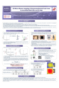
Integrated circuits and optoelectronic devices are complex systems consisting of various materials with different characteristics that can develop mechanical stress when assembled. Since the presence of local stress influences the electronic performance of the device, it is useful to investigate the presence of stress and its distribution in different samples. Micro-Raman spectroscopy allows for determination, mapping, and quantification of local stress and is a powerful tool in understanding how various assembly methods of different materials influence the stress distribution in each layer of complex electronic systems such as LEDs.
This work focusses on the Raman investigation of both metal and semiconductor material properties in integrated circuits: silicon chips that simulate part of the structure of an optoelectronic device, and GaN LEDs. Silicon chips (120 μm thick) are soldered to copper substrates. Blue GaN-based LEDs, bonded to a silicon carrier using gold silicon, are soldered with an AuSn alloy on copper substrates, with different thicknesses. Stress is determined by 2D Raman mapping of the surface, at 514.15 nm, in a wide temperature range, from -50 to 180°C: from the determination of the Raman peak position of Silicon centered around 520 cm-1, and GaN, centered around 568 cm-1, the presence of tensile and compressive stresses on the samples are evaluated.
Keywords
Integrated devices
silicon
GaN
tensile stress
compressive stress
Raman
Poster
sciforum-074696 .pdf
Valuing the ecological and socio-economic interests of the Moroccan coastal lagoons: An ecosystem services framework
Facial Beauty Prediction using an Ensemble of Deep Convolutional Neural Networks