Event submissions
Published
This submission belongs to the session S2. Nanoenergies and Nanocatalysis of the event The 5th International Online Conference on Nanomaterials
Published date
19 Sep, 2025
Academic Editor
'%3e%3cpath%20d='M12.6657%2010.9104C12.4185%2010.325%2012.0599%209.79327%2011.6097%209.34482C11.1609%208.89508%2010.6293%208.5365%2010.0442%208.28888C10.0389%208.28626%2010.0337%208.28495%2010.0285%208.28233C10.8446%207.69279%2011.3752%206.73249%2011.3752%205.64904C11.3752%203.8542%209.92103%202.39999%208.1262%202.39999C6.33136%202.39999%204.87715%203.8542%204.87715%205.64904C4.87715%206.73249%205.40774%207.69279%206.22393%208.28364C6.21869%208.28626%206.21345%208.28757%206.20821%208.29019C5.62129%208.5378%205.09463%208.89284%204.64265%209.34613C4.1929%209.79493%203.83432%2010.3266%203.58671%2010.9117C3.34345%2011.4845%203.21226%2012.0987%203.20023%2012.7209C3.19988%2012.7349%203.20233%2012.7488%203.20744%2012.7619C3.21255%2012.7749%203.22022%2012.7867%203.22998%2012.7968C3.23975%2012.8068%203.25142%2012.8147%203.26431%2012.8202C3.2772%2012.8256%203.29105%2012.8284%203.30504%2012.8284H4.09109C4.14874%2012.8284%204.19459%2012.7825%204.1959%2012.7262C4.2221%2011.7148%204.62823%2010.7676%205.34617%2010.0497C6.08899%209.30683%207.0755%208.89808%208.1262%208.89808C9.17689%208.89808%2010.1634%209.30683%2010.9062%2010.0497C11.6242%2010.7676%2012.0303%2011.7148%2012.0565%2012.7262C12.0578%2012.7838%2012.1037%2012.8284%2012.1613%2012.8284H12.9474C12.9613%2012.8284%2012.9752%2012.8256%2012.9881%2012.8202C13.001%2012.8147%2013.0126%2012.8068%2013.0224%2012.7968C13.0322%2012.7867%2013.0398%2012.7749%2013.0449%2012.7619C13.0501%2012.7488%2013.0525%2012.7349%2013.0522%2012.7209C13.0391%2012.0947%2012.9094%2011.4855%2012.6657%2010.9104ZM8.1262%207.9024C7.52486%207.9024%206.9589%207.6679%206.53312%207.24211C6.10733%206.81633%205.87283%206.25037%205.87283%205.64904C5.87283%205.0477%206.10733%204.48174%206.53312%204.05596C6.9589%203.63018%207.52486%203.39567%208.1262%203.39567C8.72753%203.39567%209.29349%203.63018%209.71927%204.05596C10.1451%204.48174%2010.3796%205.0477%2010.3796%205.64904C10.3796%206.25037%2010.1451%206.81633%209.71927%207.24211C9.29349%207.6679%208.72753%207.9024%208.1262%207.9024Z'%20fill='%235D1EE1'/%3e%3c/g%3e%3c/svg%3e) Jian-Gan Wang
Jian-Gan WangCitation
Pabina Rani Boro, Rupam Deka, Pranjal Sarmah, Partha Protim Borthakur, Nanostructured Semiconductors for Enhanced Waste Heat-to-Electricity Conversion, in Proceedings of The 5th International Online Conference on Nanomaterials, 22 September–24 September 2025, MDPI: Basel, Switzerland
Share
Email
Facebook
Twitter
LinkedIn
Nanostructured Semiconductors for Enhanced Waste Heat-to-Electricity Conversion

Pabina Rani Boro 1
'%3e%3cpath%20d='M12.6647%2010.9104C12.4176%2010.325%2012.0589%209.7933%2011.6088%209.34485C11.16%208.89511%2010.6283%208.53653%2010.0432%208.28891C10.038%208.28629%2010.0327%208.28498%2010.0275%208.28236C10.8437%207.69282%2011.3743%206.73252%2011.3743%205.64907C11.3743%203.85423%209.92005%202.40002%208.12522%202.40002C6.33038%202.40002%204.87618%203.85423%204.87618%205.64907C4.87618%206.73252%205.40677%207.69282%206.22296%208.28367C6.21772%208.28629%206.21248%208.2876%206.20724%208.29022C5.62031%208.53783%205.09365%208.89287%204.64167%209.34616C4.19192%209.79496%203.83334%2010.3266%203.58573%2010.9117C3.34247%2011.4846%203.21128%2012.0987%203.19925%2012.721C3.1989%2012.735%203.20135%2012.7489%203.20646%2012.7619C3.21157%2012.7749%203.21924%2012.7868%203.22901%2012.7968C3.23877%2012.8068%203.25045%2012.8148%203.26334%2012.8202C3.27623%2012.8256%203.29007%2012.8284%203.30406%2012.8284H4.09012C4.14776%2012.8284%204.19362%2012.7825%204.19493%2012.7262C4.22113%2011.7148%204.62726%2010.7676%205.34519%2010.0497C6.08802%209.30686%207.07452%208.89811%208.12522%208.89811C9.17592%208.89811%2010.1624%209.30686%2010.9052%2010.0497C11.6232%2010.7676%2012.0293%2011.7148%2012.0555%2012.7262C12.0568%2012.7839%2012.1027%2012.8284%2012.1603%2012.8284H12.9464C12.9604%2012.8284%2012.9742%2012.8256%2012.9871%2012.8202C13%2012.8148%2013.0117%2012.8068%2013.0214%2012.7968C13.0312%2012.7868%2013.0389%2012.7749%2013.044%2012.7619C13.0491%2012.7489%2013.0515%2012.735%2013.0512%2012.721C13.0381%2012.0947%2012.9084%2011.4856%2012.6647%2010.9104ZM8.12522%207.90243C7.52388%207.90243%206.95792%207.66793%206.53214%207.24215C6.10636%206.81636%205.87185%206.2504%205.87185%205.64907C5.87185%205.04773%206.10636%204.48177%206.53214%204.05599C6.95792%203.63021%207.52388%203.3957%208.12522%203.3957C8.72655%203.3957%209.29252%203.63021%209.7183%204.05599C10.1441%204.48177%2010.3786%205.04773%2010.3786%205.64907C10.3786%206.2504%2010.1441%206.81636%209.7183%207.24215C9.29252%207.66793%208.72655%207.90243%208.12522%207.90243Z'%20fill='%235D1EE1'/%3e%3c/g%3e%3c/svg%3e)
Rupam Deka 1
Pranjal Sarmah 1

Partha Protim Borthakur 1
1. Department of Mechanical Engineering, Dibrugarh University, Dibrugarh, Assam 786004, India
Abstract
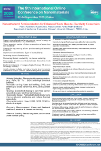
Nanostructured semiconductors have emerged as transformative materials for enhancing the efficiency of waste heat-to-electricity conversion through thermoelectric (TE) processes. By altering structural features at the nanoscale, these materials can simultaneously reduce lattice thermal conductivity and optimize electronic transport properties, thereby significantly improving the thermoelectric figure of merit (ZT). Recent studies have demonstrated that introducing periodic twin planes in III-V semiconductor nanowires can achieve a tenfold reduction in thermal conductivity while maintaining excellent electrical performance. Similarly, Pb₁₋ₓGeₓTe alloys, through controlled spinodal decomposition, form stable nanostructures that maintain low thermal conductivity even after undergoing thermal cycling, which is crucial for high-temperature applications. Enhancing electrical properties is another key advantage of nanostructuring. PbTe-based materials, when heavily doped and engineered with nanoscale inclusions, have achieved a ZT of approximately 1.9 and a thermoelectric efficiency of around 12% over a 590 K temperature difference. Single-walled carbon nanotubes (SWCNTs) exhibit strong correlations between their electronic structure and thermoelectric conductivity, highlighting their potential for next-generation devices. Two-dimensional silicon–germanium (SiₓGeᵧ) compounds offer ultra-low lattice thermal conductivity and high Seebeck coefficients, providing a promising pathway for future TE applications. Despite these advancements, challenges remain, particularly regarding scalability and integration into existing energy recovery systems. Techniques such as focused ion beam milling and solution-based synthesis of porous nanostructures are being developed to fabricate high-performance materials on a commercial scale. Moreover, integrating nanostructured semiconductors into real-world systems, such as automotive exhaust heat recovery units, requires improvements in material durability, fabrication efficiency, and device compatibility. In conclusion, nanostructured semiconductors offer a powerful route for enhancing waste heat-to-electricity conversion. Their ability to decouple electrical and thermal transport at the nanoscale opens new opportunities for high-efficiency, sustainable energy harvesting technologies. Continued research into scalable manufacturing techniques, material stability, and system integration is essential to fully unlock their potential for commercial thermoelectric applications
Keywords
Nanostructured Semiconductors
Thermoelectric Materials
Waste Heat Recovery
Thermal Conductivity Reduction
Silicon-Germanium Nanostructures.
Poster
sciforum-123696.pdf
Antimicrobial activity of green-synthesized Pr doped zinc oxide nanoparticles
MXene as a multi-functional 2D reinforcement in self-lubricating PEEK-based composites