Event submissions
Published
This submission belongs to the session S1. Optical, Electric and Magnetic Materials and Their Characterization of the event The 4th International Online Conference on Materials
Published date
29 Oct, 2025
Academic Editor
'%3e%3cpath%20d='M12.6657%2010.9104C12.4185%2010.325%2012.0599%209.79327%2011.6097%209.34482C11.1609%208.89508%2010.6293%208.5365%2010.0442%208.28888C10.0389%208.28626%2010.0337%208.28495%2010.0285%208.28233C10.8446%207.69279%2011.3752%206.73249%2011.3752%205.64904C11.3752%203.8542%209.92103%202.39999%208.1262%202.39999C6.33136%202.39999%204.87715%203.8542%204.87715%205.64904C4.87715%206.73249%205.40774%207.69279%206.22393%208.28364C6.21869%208.28626%206.21345%208.28757%206.20821%208.29019C5.62129%208.5378%205.09463%208.89284%204.64265%209.34613C4.1929%209.79493%203.83432%2010.3266%203.58671%2010.9117C3.34345%2011.4845%203.21226%2012.0987%203.20023%2012.7209C3.19988%2012.7349%203.20233%2012.7488%203.20744%2012.7619C3.21255%2012.7749%203.22022%2012.7867%203.22998%2012.7968C3.23975%2012.8068%203.25142%2012.8147%203.26431%2012.8202C3.2772%2012.8256%203.29105%2012.8284%203.30504%2012.8284H4.09109C4.14874%2012.8284%204.19459%2012.7825%204.1959%2012.7262C4.2221%2011.7148%204.62823%2010.7676%205.34617%2010.0497C6.08899%209.30683%207.0755%208.89808%208.1262%208.89808C9.17689%208.89808%2010.1634%209.30683%2010.9062%2010.0497C11.6242%2010.7676%2012.0303%2011.7148%2012.0565%2012.7262C12.0578%2012.7838%2012.1037%2012.8284%2012.1613%2012.8284H12.9474C12.9613%2012.8284%2012.9752%2012.8256%2012.9881%2012.8202C13.001%2012.8147%2013.0126%2012.8068%2013.0224%2012.7968C13.0322%2012.7867%2013.0398%2012.7749%2013.0449%2012.7619C13.0501%2012.7488%2013.0525%2012.7349%2013.0522%2012.7209C13.0391%2012.0947%2012.9094%2011.4855%2012.6657%2010.9104ZM8.1262%207.9024C7.52486%207.9024%206.9589%207.6679%206.53312%207.24211C6.10733%206.81633%205.87283%206.25037%205.87283%205.64904C5.87283%205.0477%206.10733%204.48174%206.53312%204.05596C6.9589%203.63018%207.52486%203.39567%208.1262%203.39567C8.72753%203.39567%209.29349%203.63018%209.71927%204.05596C10.1451%204.48174%2010.3796%205.0477%2010.3796%205.64904C10.3796%206.25037%2010.1451%206.81633%209.71927%207.24211C9.29349%207.6679%208.72753%207.9024%208.1262%207.9024Z'%20fill='%235D1EE1'/%3e%3c/g%3e%3c/svg%3e) Weili Zhang
Weili ZhangCitation
Andrii Kashuba, Hryhorii Ilchuk, Vasyl Kordan, Ihor Semkiv, Myron Rudysh, Mykola Solovyov, Effect of deposition time on the optical properties of CdSe nanostructured films, in Proceedings of The 4th International Online Conference on Materials, 3 November–6 November 2025, MDPI: Basel, Switzerland
Share
Email
Facebook
Twitter
LinkedIn
Effect of deposition time on the optical properties of CdSe nanostructured films
'%3e%3cpath%20d='M12.6647%2010.9104C12.4176%2010.325%2012.0589%209.7933%2011.6088%209.34485C11.16%208.89511%2010.6283%208.53653%2010.0432%208.28891C10.038%208.28629%2010.0327%208.28498%2010.0275%208.28236C10.8437%207.69282%2011.3743%206.73252%2011.3743%205.64907C11.3743%203.85423%209.92005%202.40002%208.12522%202.40002C6.33038%202.40002%204.87618%203.85423%204.87618%205.64907C4.87618%206.73252%205.40677%207.69282%206.22296%208.28367C6.21772%208.28629%206.21248%208.2876%206.20724%208.29022C5.62031%208.53783%205.09365%208.89287%204.64167%209.34616C4.19192%209.79496%203.83334%2010.3266%203.58573%2010.9117C3.34247%2011.4846%203.21128%2012.0987%203.19925%2012.721C3.1989%2012.735%203.20135%2012.7489%203.20646%2012.7619C3.21157%2012.7749%203.21924%2012.7868%203.22901%2012.7968C3.23877%2012.8068%203.25045%2012.8148%203.26334%2012.8202C3.27623%2012.8256%203.29007%2012.8284%203.30406%2012.8284H4.09012C4.14776%2012.8284%204.19362%2012.7825%204.19493%2012.7262C4.22113%2011.7148%204.62726%2010.7676%205.34519%2010.0497C6.08802%209.30686%207.07452%208.89811%208.12522%208.89811C9.17592%208.89811%2010.1624%209.30686%2010.9052%2010.0497C11.6232%2010.7676%2012.0293%2011.7148%2012.0555%2012.7262C12.0568%2012.7839%2012.1027%2012.8284%2012.1603%2012.8284H12.9464C12.9604%2012.8284%2012.9742%2012.8256%2012.9871%2012.8202C13%2012.8148%2013.0117%2012.8068%2013.0214%2012.7968C13.0312%2012.7868%2013.0389%2012.7749%2013.044%2012.7619C13.0491%2012.7489%2013.0515%2012.735%2013.0512%2012.721C13.0381%2012.0947%2012.9084%2011.4856%2012.6647%2010.9104ZM8.12522%207.90243C7.52388%207.90243%206.95792%207.66793%206.53214%207.24215C6.10636%206.81636%205.87185%206.2504%205.87185%205.64907C5.87185%205.04773%206.10636%204.48177%206.53214%204.05599C6.95792%203.63021%207.52388%203.3957%208.12522%203.3957C8.72655%203.3957%209.29252%203.63021%209.7183%204.05599C10.1441%204.48177%2010.3786%205.04773%2010.3786%205.64907C10.3786%206.2504%2010.1441%206.81636%209.7183%207.24215C9.29252%207.66793%208.72655%207.90243%208.12522%207.90243Z'%20fill='%235D1EE1'/%3e%3c/g%3e%3c/svg%3e)
Andrii Kashuba 1
Hryhorii Ilchuk 1
Vasyl Kordan 2
Ihor Semkiv 1
Myron Rudysh 2
Mykola Solovyov 1
1. Lviv Polytechnic National University, Bandera Str. 12, 79013 Lviv, Ukraine
2. Ivan Franko National University of Lviv, Kyrylo & Mephodiy Str. 8, 79000 Lviv, Ukraine
Abstract
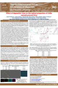
Cadmium selenide nanostructured films were prepared using the high-frequency (HF) magnetron sputtering method. All samples were deposited on quartz substrates in disk form with a radius of 16 mm. The temperature of the substrate was maintained at 180 °C for all samples. The deposition times were 3, 6, 9, 12 and 20 min. The effect of deposition time on the optical properties of CdSe nanostructured films was investigated by X-ray diffraction (XRD), optical absorption spectra (OAS), a scanning electron microscope (SEM) and an energy-dispersive X-ray analyser (EDX). XRD analysis of the obtained samples exhibited a cubic structure with a preferred (200) orientation. The average crystallite size of the CdSe nanostructured films was determined using the Scherrer equation. An increase in deposition time was found to result in a corresponding increase in crystallite size. The EDX showed that the CdSe nanostructured films were formed from the desired elements, and their distribution was uniform. SEM analysis showed that the surface morphologies of the CdSe nanostructured films were dependent on the deposition time. OAS was analysed using the Tauc model. The absorption spectrum fitting (ASF) method was applied to estimate the optical band gap and Urbach energy of the CdSe nanostructured films. The optical band gap and Urbach energy were found to decrease with increasing deposition time. This behavior is ascribed to the growth in particle size.
Keywords
cadmium selenide
AIIBVI
band gap
Urbach energy
absorption spectra
Poster
sciforum-142184.pdf
Effect of Surface Printing on the Release Kinetics of Gentamicin from Gradient Samples for Bone Applications
Relationship between biopolymer properties