Event submissions
Published
This submission belongs to the session S4. Electrical, Electronics and Communications Engineering of the event The 6th International Electronic Conference on Applied Sciences
Published date
03 Dec, 2025
Academic Editor
'%3e%3cpath%20d='M12.6657%2010.9104C12.4185%2010.325%2012.0599%209.79327%2011.6097%209.34482C11.1609%208.89508%2010.6293%208.5365%2010.0442%208.28888C10.0389%208.28626%2010.0337%208.28495%2010.0285%208.28233C10.8446%207.69279%2011.3752%206.73249%2011.3752%205.64904C11.3752%203.8542%209.92103%202.39999%208.1262%202.39999C6.33136%202.39999%204.87715%203.8542%204.87715%205.64904C4.87715%206.73249%205.40774%207.69279%206.22393%208.28364C6.21869%208.28626%206.21345%208.28757%206.20821%208.29019C5.62129%208.5378%205.09463%208.89284%204.64265%209.34613C4.1929%209.79493%203.83432%2010.3266%203.58671%2010.9117C3.34345%2011.4845%203.21226%2012.0987%203.20023%2012.7209C3.19988%2012.7349%203.20233%2012.7488%203.20744%2012.7619C3.21255%2012.7749%203.22022%2012.7867%203.22998%2012.7968C3.23975%2012.8068%203.25142%2012.8147%203.26431%2012.8202C3.2772%2012.8256%203.29105%2012.8284%203.30504%2012.8284H4.09109C4.14874%2012.8284%204.19459%2012.7825%204.1959%2012.7262C4.2221%2011.7148%204.62823%2010.7676%205.34617%2010.0497C6.08899%209.30683%207.0755%208.89808%208.1262%208.89808C9.17689%208.89808%2010.1634%209.30683%2010.9062%2010.0497C11.6242%2010.7676%2012.0303%2011.7148%2012.0565%2012.7262C12.0578%2012.7838%2012.1037%2012.8284%2012.1613%2012.8284H12.9474C12.9613%2012.8284%2012.9752%2012.8256%2012.9881%2012.8202C13.001%2012.8147%2013.0126%2012.8068%2013.0224%2012.7968C13.0322%2012.7867%2013.0398%2012.7749%2013.0449%2012.7619C13.0501%2012.7488%2013.0525%2012.7349%2013.0522%2012.7209C13.0391%2012.0947%2012.9094%2011.4855%2012.6657%2010.9104ZM8.1262%207.9024C7.52486%207.9024%206.9589%207.6679%206.53312%207.24211C6.10733%206.81633%205.87283%206.25037%205.87283%205.64904C5.87283%205.0477%206.10733%204.48174%206.53312%204.05596C6.9589%203.63018%207.52486%203.39567%208.1262%203.39567C8.72753%203.39567%209.29349%203.63018%209.71927%204.05596C10.1451%204.48174%2010.3796%205.0477%2010.3796%205.64904C10.3796%206.25037%2010.1451%206.81633%209.71927%207.24211C9.29349%207.6679%208.72753%207.9024%208.1262%207.9024Z'%20fill='%235D1EE1'/%3e%3c/g%3e%3c/svg%3e) Alessandro Lo Schiavo
Alessandro Lo SchiavoCitation
Pallabi Pahari, S K Mohapatra, J K Das, O P Acharya, Exploring the Impact of Key Design Parameters on Double-Gate TFET Performance for Low-Power Applications, in Proceedings of The 6th International Electronic Conference on Applied Sciences, 9 December–11 December 2025, MDPI: Basel, Switzerland
Share
Email
Facebook
Twitter
LinkedIn
Exploring the Impact of Key Design Parameters on Double-Gate TFET Performance for Low-Power Applications
'%3e%3cpath%20d='M12.6647%2010.9104C12.4176%2010.325%2012.0589%209.7933%2011.6088%209.34485C11.16%208.89511%2010.6283%208.53653%2010.0432%208.28891C10.038%208.28629%2010.0327%208.28498%2010.0275%208.28236C10.8437%207.69282%2011.3743%206.73252%2011.3743%205.64907C11.3743%203.85423%209.92005%202.40002%208.12522%202.40002C6.33038%202.40002%204.87618%203.85423%204.87618%205.64907C4.87618%206.73252%205.40677%207.69282%206.22296%208.28367C6.21772%208.28629%206.21248%208.2876%206.20724%208.29022C5.62031%208.53783%205.09365%208.89287%204.64167%209.34616C4.19192%209.79496%203.83334%2010.3266%203.58573%2010.9117C3.34247%2011.4846%203.21128%2012.0987%203.19925%2012.721C3.1989%2012.735%203.20135%2012.7489%203.20646%2012.7619C3.21157%2012.7749%203.21924%2012.7868%203.22901%2012.7968C3.23877%2012.8068%203.25045%2012.8148%203.26334%2012.8202C3.27623%2012.8256%203.29007%2012.8284%203.30406%2012.8284H4.09012C4.14776%2012.8284%204.19362%2012.7825%204.19493%2012.7262C4.22113%2011.7148%204.62726%2010.7676%205.34519%2010.0497C6.08802%209.30686%207.07452%208.89811%208.12522%208.89811C9.17592%208.89811%2010.1624%209.30686%2010.9052%2010.0497C11.6232%2010.7676%2012.0293%2011.7148%2012.0555%2012.7262C12.0568%2012.7839%2012.1027%2012.8284%2012.1603%2012.8284H12.9464C12.9604%2012.8284%2012.9742%2012.8256%2012.9871%2012.8202C13%2012.8148%2013.0117%2012.8068%2013.0214%2012.7968C13.0312%2012.7868%2013.0389%2012.7749%2013.044%2012.7619C13.0491%2012.7489%2013.0515%2012.735%2013.0512%2012.721C13.0381%2012.0947%2012.9084%2011.4856%2012.6647%2010.9104ZM8.12522%207.90243C7.52388%207.90243%206.95792%207.66793%206.53214%207.24215C6.10636%206.81636%205.87185%206.2504%205.87185%205.64907C5.87185%205.04773%206.10636%204.48177%206.53214%204.05599C6.95792%203.63021%207.52388%203.3957%208.12522%203.3957C8.72655%203.3957%209.29252%203.63021%209.7183%204.05599C10.1441%204.48177%2010.3786%205.04773%2010.3786%205.64907C10.3786%206.2504%2010.1441%206.81636%209.7183%207.24215C9.29252%207.66793%208.72655%207.90243%208.12522%207.90243Z'%20fill='%235D1EE1'/%3e%3c/g%3e%3c/svg%3e)
Pallabi Pahari 1
S K Mohapatra 1
J K Das 1
O P Acharya 1
1. School of Electronics Engineering, Kalinga Institute of Industrial Technology (KIIT) Deemed to be University, Bhubaneswar, India
Abstract
Tunnel Field-Effect Transistors (TFETs) are being widely explored for ultra-low-power VLSI because their band-to-band tunnelling (BTBT) transport permits subthreshold swings (SSs) below the 60 mV/dec thermionic limit at room temperature, along with significantly lower leakage than MOSFETs. This paper presents a systematic TCAD study of Double-Gate (DG) TFETs, which maps how four primary knobs—gate dielectric material, silicon channel thickness, gate length, and source and drain doping—shape the following key figures of merit: ON-current (ION), OFF-current (IOFF), threshold voltage (VTH), SS, and the ION/IOFF switching ratio. High-κ gate enhances gate-to-channel coupling and boosts tunnelling efficiency; rigorous body scaling enhances electrostatic control; and targeted source-proximal doping profiles elevate ION while minimising leakage. We also measure the trade-offs between ION, SS, and IOFF that occur when scaling is completed at the same time. This shows that careful coordination is needed instead of simply tuning one parameter. This is a simulated work; the physical models are calibrated to experimental TFET data, and all parameters were checked against previously reported results. The device reaches SS = 31.4 mV/dec, VTH = 0.46 V, ION = 5.91 × 10⁻⁵ A, and an ION/IOFF of about 4.5 × 10¹¹. This shows that it can switch quickly with little leakage. The design insights that come from this work can provide useful advice on how to choose gate dielectric materials, structures, and doping strategies so that DG-TFETs can be included in the next generation of low-power semiconductor technologies.
Keywords
Double-Gate TFET (DG-TFET)
Low-power electronics
Band-to-band tunnelling
Subthreshold swing
High-k dielectric
Channel thickness scaling
Doping optimization
Poster
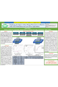
Pallabi Poster presentation Dec 2025.pdf
Modeling a microgrid based on the IEC-61850 architecture using Petri Nets
Real-Time Emotion-Based Concentration Estimation: An Educational Framework with Lightweight Neural Networks