Event submissions
Published
This submission belongs to the session S2. Advanced sustainable energy conversion systems of the event The 1st International Online Conference on Inventions
Published date
22 Jun, 2026
Academic Editor
'%3e%3cpath%20d='M12.6657%2010.9104C12.4185%2010.325%2012.0599%209.79327%2011.6097%209.34482C11.1609%208.89508%2010.6293%208.5365%2010.0442%208.28888C10.0389%208.28626%2010.0337%208.28495%2010.0285%208.28233C10.8446%207.69279%2011.3752%206.73249%2011.3752%205.64904C11.3752%203.8542%209.92103%202.39999%208.1262%202.39999C6.33136%202.39999%204.87715%203.8542%204.87715%205.64904C4.87715%206.73249%205.40774%207.69279%206.22393%208.28364C6.21869%208.28626%206.21345%208.28757%206.20821%208.29019C5.62129%208.5378%205.09463%208.89284%204.64265%209.34613C4.1929%209.79493%203.83432%2010.3266%203.58671%2010.9117C3.34345%2011.4845%203.21226%2012.0987%203.20023%2012.7209C3.19988%2012.7349%203.20233%2012.7488%203.20744%2012.7619C3.21255%2012.7749%203.22022%2012.7867%203.22998%2012.7968C3.23975%2012.8068%203.25142%2012.8147%203.26431%2012.8202C3.2772%2012.8256%203.29105%2012.8284%203.30504%2012.8284H4.09109C4.14874%2012.8284%204.19459%2012.7825%204.1959%2012.7262C4.2221%2011.7148%204.62823%2010.7676%205.34617%2010.0497C6.08899%209.30683%207.0755%208.89808%208.1262%208.89808C9.17689%208.89808%2010.1634%209.30683%2010.9062%2010.0497C11.6242%2010.7676%2012.0303%2011.7148%2012.0565%2012.7262C12.0578%2012.7838%2012.1037%2012.8284%2012.1613%2012.8284H12.9474C12.9613%2012.8284%2012.9752%2012.8256%2012.9881%2012.8202C13.001%2012.8147%2013.0126%2012.8068%2013.0224%2012.7968C13.0322%2012.7867%2013.0398%2012.7749%2013.0449%2012.7619C13.0501%2012.7488%2013.0525%2012.7349%2013.0522%2012.7209C13.0391%2012.0947%2012.9094%2011.4855%2012.6657%2010.9104ZM8.1262%207.9024C7.52486%207.9024%206.9589%207.6679%206.53312%207.24211C6.10733%206.81633%205.87283%206.25037%205.87283%205.64904C5.87283%205.0477%206.10733%204.48174%206.53312%204.05596C6.9589%203.63018%207.52486%203.39567%208.1262%203.39567C8.72753%203.39567%209.29349%203.63018%209.71927%204.05596C10.1451%204.48174%2010.3796%205.0477%2010.3796%205.64904C10.3796%206.25037%2010.1451%206.81633%209.71927%207.24211C9.29349%207.6679%208.72753%207.9024%208.1262%207.9024Z'%20fill='%235D1EE1'/%3e%3c/g%3e%3c/svg%3e) Said Al-Hallaj
Said Al-HallajCitation
Isuranga Sandun Abejeewa, Vikum Premalal, Manel Sarangika, Kaveenga Rasika Koswattage, Lakshan Priyankara, Lasitha Madhusanka, Process Optimization of Copper Antimony Sulfide Thin Films via Chemical Bath Deposition for High-Performance Photovoltaic Applications., in Proceedings of The 1st International Online Conference on Inventions, 25 June–26 June 2026, MDPI: Basel, Switzerland
Share
Email
Facebook
Twitter
LinkedIn
Process Optimization of Copper Antimony Sulfide Thin Films via Chemical Bath Deposition for High-Performance Photovoltaic Applications.
'%3e%3cpath%20d='M12.6647%2010.9104C12.4176%2010.325%2012.0589%209.7933%2011.6088%209.34485C11.16%208.89511%2010.6283%208.53653%2010.0432%208.28891C10.038%208.28629%2010.0327%208.28498%2010.0275%208.28236C10.8437%207.69282%2011.3743%206.73252%2011.3743%205.64907C11.3743%203.85423%209.92005%202.40002%208.12522%202.40002C6.33038%202.40002%204.87618%203.85423%204.87618%205.64907C4.87618%206.73252%205.40677%207.69282%206.22296%208.28367C6.21772%208.28629%206.21248%208.2876%206.20724%208.29022C5.62031%208.53783%205.09365%208.89287%204.64167%209.34616C4.19192%209.79496%203.83334%2010.3266%203.58573%2010.9117C3.34247%2011.4846%203.21128%2012.0987%203.19925%2012.721C3.1989%2012.735%203.20135%2012.7489%203.20646%2012.7619C3.21157%2012.7749%203.21924%2012.7868%203.22901%2012.7968C3.23877%2012.8068%203.25045%2012.8148%203.26334%2012.8202C3.27623%2012.8256%203.29007%2012.8284%203.30406%2012.8284H4.09012C4.14776%2012.8284%204.19362%2012.7825%204.19493%2012.7262C4.22113%2011.7148%204.62726%2010.7676%205.34519%2010.0497C6.08802%209.30686%207.07452%208.89811%208.12522%208.89811C9.17592%208.89811%2010.1624%209.30686%2010.9052%2010.0497C11.6232%2010.7676%2012.0293%2011.7148%2012.0555%2012.7262C12.0568%2012.7839%2012.1027%2012.8284%2012.1603%2012.8284H12.9464C12.9604%2012.8284%2012.9742%2012.8256%2012.9871%2012.8202C13%2012.8148%2013.0117%2012.8068%2013.0214%2012.7968C13.0312%2012.7868%2013.0389%2012.7749%2013.044%2012.7619C13.0491%2012.7489%2013.0515%2012.735%2013.0512%2012.721C13.0381%2012.0947%2012.9084%2011.4856%2012.6647%2010.9104ZM8.12522%207.90243C7.52388%207.90243%206.95792%207.66793%206.53214%207.24215C6.10636%206.81636%205.87185%206.2504%205.87185%205.64907C5.87185%205.04773%206.10636%204.48177%206.53214%204.05599C6.95792%203.63021%207.52388%203.3957%208.12522%203.3957C8.72655%203.3957%209.29252%203.63021%209.7183%204.05599C10.1441%204.48177%2010.3786%205.04773%2010.3786%205.64907C10.3786%206.2504%2010.1441%206.81636%209.7183%207.24215C9.29252%207.66793%208.72655%207.90243%208.12522%207.90243Z'%20fill='%235D1EE1'/%3e%3c/g%3e%3c/svg%3e)
Isuranga Sandun Abejeewa 1
Vikum Premalal 2
Manel Sarangika 3
Kaveenga Rasika Koswattage 4
Lakshan Priyankara 4

Lasitha Madhusanka 4
1. Faculty of Graduate Studies, Sabaragamuwa University of Sri Lanka, Belihuloya, Sri Lanka
2. Faculty of Technology, University of Jayewardenepura, Nugegoda, Sri Lanka
3. Department of Physical science and Technology, Faculty of Applied Sciences, Sabaragamuwa University, Belihuloya, Sri Lanka
4. Faculty of Technology, Sabaragamuwa University of Sri Lanka, Belihuloya, Sri Lanka
Abstract
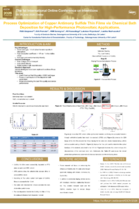
Copper antimony sulfide (CuSbS₂) has the potential to be an excellent absorber material for thin-film solar cells. It has an optimal direct band gap of 1.5 eV, strong absorption coefficients >10⁴ cm⁻¹, and is composed of non-toxic and earth-abundant elements. However, the difficulty in growing properly stoichiometric and well-crystallized CuSbS₂ thin films by chemical bath deposition remains. This work aims to optimize the CBD conditions for the deposition of CuSbS₂ thin films by enhancing the uniformity, crystallinity, and optical quality of the material, which are critical for its application in solar cells. TiO₂ electron transport layers on FTO glass substrates were prepared by the doctor blade technique. This technique provided a smooth surface for the CuSbS₂ thin film, which adhered properly. The CuSbS₂ thin film was prepared by dissolving SbCl₃ in acetone, Na₂S₂O₃, and CuCl₂ in a precursor solution. The thin film was then deposited at room temperature for 3 hours in a 50 ml bath. Solar cell architecture is described as follows: FTO/TiO₂/CuSbS₂/CuI/Pt-glass. The XRD patterns show the proper formation of the orthorhombic chalcocite CuSbS₂ phase. The strong (111) peak indicates the high crystallinity of the CuSbS₂ thin film. The scanning electron microscope (SEM) showed densely packed grains with minimal void spaces, indicating good surface coverage. The optical measurements, which included UV-Vis spectroscopy and Tauc plots, showed a direct band gap of 1.6 eV, which is optimal for solar energy absorption. The current research has shown that with optimized CBD conditions, good-quality CuSbS₂ films can be deposited, which is useful for efficient and sustainable solar energy conversion.
Keywords
Band Gap Tuning
Chemical Bath Deposition
Solar Cell Applications
Thin Films.
Poster
MDPI Conference Poster.pdf
Experimental analysis of single-slope solar still equipped with jute and nano-enhanced jute cloth for clean water production
Adaptive Maximum Power Point Tracking Technique for Standalone PV Systems