Event submissions
Published
This submission belongs to the session S6. Energy Systems of the event The 5th International Electronic Conference on Processes
Published date
15 Oct, 2026
Academic Editor
'%3e%3cpath%20d='M12.6657%2010.9104C12.4185%2010.325%2012.0599%209.79327%2011.6097%209.34482C11.1609%208.89508%2010.6293%208.5365%2010.0442%208.28888C10.0389%208.28626%2010.0337%208.28495%2010.0285%208.28233C10.8446%207.69279%2011.3752%206.73249%2011.3752%205.64904C11.3752%203.8542%209.92103%202.39999%208.1262%202.39999C6.33136%202.39999%204.87715%203.8542%204.87715%205.64904C4.87715%206.73249%205.40774%207.69279%206.22393%208.28364C6.21869%208.28626%206.21345%208.28757%206.20821%208.29019C5.62129%208.5378%205.09463%208.89284%204.64265%209.34613C4.1929%209.79493%203.83432%2010.3266%203.58671%2010.9117C3.34345%2011.4845%203.21226%2012.0987%203.20023%2012.7209C3.19988%2012.7349%203.20233%2012.7488%203.20744%2012.7619C3.21255%2012.7749%203.22022%2012.7867%203.22998%2012.7968C3.23975%2012.8068%203.25142%2012.8147%203.26431%2012.8202C3.2772%2012.8256%203.29105%2012.8284%203.30504%2012.8284H4.09109C4.14874%2012.8284%204.19459%2012.7825%204.1959%2012.7262C4.2221%2011.7148%204.62823%2010.7676%205.34617%2010.0497C6.08899%209.30683%207.0755%208.89808%208.1262%208.89808C9.17689%208.89808%2010.1634%209.30683%2010.9062%2010.0497C11.6242%2010.7676%2012.0303%2011.7148%2012.0565%2012.7262C12.0578%2012.7838%2012.1037%2012.8284%2012.1613%2012.8284H12.9474C12.9613%2012.8284%2012.9752%2012.8256%2012.9881%2012.8202C13.001%2012.8147%2013.0126%2012.8068%2013.0224%2012.7968C13.0322%2012.7867%2013.0398%2012.7749%2013.0449%2012.7619C13.0501%2012.7488%2013.0525%2012.7349%2013.0522%2012.7209C13.0391%2012.0947%2012.9094%2011.4855%2012.6657%2010.9104ZM8.1262%207.9024C7.52486%207.9024%206.9589%207.6679%206.53312%207.24211C6.10733%206.81633%205.87283%206.25037%205.87283%205.64904C5.87283%205.0477%206.10733%204.48174%206.53312%204.05596C6.9589%203.63018%207.52486%203.39567%208.1262%203.39567C8.72753%203.39567%209.29349%203.63018%209.71927%204.05596C10.1451%204.48174%2010.3796%205.0477%2010.3796%205.64904C10.3796%206.25037%2010.1451%206.81633%209.71927%207.24211C9.29349%207.6679%208.72753%207.9024%208.1262%207.9024Z'%20fill='%235D1EE1'/%3e%3c/g%3e%3c/svg%3e) Blaž Likozar
Blaž LikozarCitation
Ahmed Bahaeddine Bensedira, abdelghani boucheham, Ouail Imed Eddine SOLTANE, Abbes Marref, Boutaleb Labdelli, Oussama Djema, Kheira Bekhedda, Abdelkader Djelloul, Effect of Drive-In Temperature and N₂/O₂ Gas Flow on Boron Diffusion Profiles in p⁺ Emitters for n-Type PERT Silicon Solar Cells, in Proceedings of The 5th International Electronic Conference on Processes, 20 October–22 October 2026, MDPI: Basel, Switzerland
Share
Email
Facebook
Twitter
LinkedIn
Effect of Drive-In Temperature and N₂/O₂ Gas Flow on Boron Diffusion Profiles in p⁺ Emitters for n-Type PERT Silicon Solar Cells
'%3e%3cpath%20d='M12.6647%2010.9104C12.4176%2010.325%2012.0589%209.7933%2011.6088%209.34485C11.16%208.89511%2010.6283%208.53653%2010.0432%208.28891C10.038%208.28629%2010.0327%208.28498%2010.0275%208.28236C10.8437%207.69282%2011.3743%206.73252%2011.3743%205.64907C11.3743%203.85423%209.92005%202.40002%208.12522%202.40002C6.33038%202.40002%204.87618%203.85423%204.87618%205.64907C4.87618%206.73252%205.40677%207.69282%206.22296%208.28367C6.21772%208.28629%206.21248%208.2876%206.20724%208.29022C5.62031%208.53783%205.09365%208.89287%204.64167%209.34616C4.19192%209.79496%203.83334%2010.3266%203.58573%2010.9117C3.34247%2011.4846%203.21128%2012.0987%203.19925%2012.721C3.1989%2012.735%203.20135%2012.7489%203.20646%2012.7619C3.21157%2012.7749%203.21924%2012.7868%203.22901%2012.7968C3.23877%2012.8068%203.25045%2012.8148%203.26334%2012.8202C3.27623%2012.8256%203.29007%2012.8284%203.30406%2012.8284H4.09012C4.14776%2012.8284%204.19362%2012.7825%204.19493%2012.7262C4.22113%2011.7148%204.62726%2010.7676%205.34519%2010.0497C6.08802%209.30686%207.07452%208.89811%208.12522%208.89811C9.17592%208.89811%2010.1624%209.30686%2010.9052%2010.0497C11.6232%2010.7676%2012.0293%2011.7148%2012.0555%2012.7262C12.0568%2012.7839%2012.1027%2012.8284%2012.1603%2012.8284H12.9464C12.9604%2012.8284%2012.9742%2012.8256%2012.9871%2012.8202C13%2012.8148%2013.0117%2012.8068%2013.0214%2012.7968C13.0312%2012.7868%2013.0389%2012.7749%2013.044%2012.7619C13.0491%2012.7489%2013.0515%2012.735%2013.0512%2012.721C13.0381%2012.0947%2012.9084%2011.4856%2012.6647%2010.9104ZM8.12522%207.90243C7.52388%207.90243%206.95792%207.66793%206.53214%207.24215C6.10636%206.81636%205.87185%206.2504%205.87185%205.64907C5.87185%205.04773%206.10636%204.48177%206.53214%204.05599C6.95792%203.63021%207.52388%203.3957%208.12522%203.3957C8.72655%203.3957%209.29252%203.63021%209.7183%204.05599C10.1441%204.48177%2010.3786%205.04773%2010.3786%205.64907C10.3786%206.2504%2010.1441%206.81636%209.7183%207.24215C9.29252%207.66793%208.72655%207.90243%208.12522%207.90243Z'%20fill='%235D1EE1'/%3e%3c/g%3e%3c/svg%3e)
Ahmed Bahaeddine Bensedira 1
abdelghani boucheham 2
Ouail Imed Eddine SOLTANE 3
Abbes Marref 2
Boutaleb Labdelli 2
Oussama Djema 2
Kheira Bekhedda 2
Abdelkader Djelloul 2
1. Department of mechanical engineering, LMP2M, Yahia Fares University, Médéa, Algeria
2. Research Center in Semiconductors Technology for Energetics (CRTSE), Semiconductor's Conversion Devices Division (DDCS), Algiers, 16038, Algeria
3. Materials Engineering (Photovoltaic and solar energy), Ecole Nationale Polytechnique de Constantine (ENPC), Constantine , 25001, Algeria
Abstract
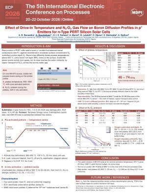
The realization of high-efficiency passivated emitter and rear totally diffused (PERT) solar cells on n-type silicon substrates requires precise control of the boron-doped p⁺ emitter. In this work, we investigate the effect of drive-in temperature on the electrical and structural properties of boron emitters formed by a two-step diffusion process using a boron nitride (BN) solid source. Seven samples were processed at drive-in temperatures ranging from 890°C to 1000°C, and their carrier concentration depth profiles were characterized by electrochemical capacitance-voltage (ECV) measurements.
The results show a strong dependence of both junction depth and surface concentration on drive-in temperature. Increasing the temperature from 890°C to 1000°C leads to a progressive deepening of the p-n junction from approximately 0.5 µm to 0.88 µm, accompanied by a reduction in sheet resistance from 74 Ω/sq down to 23 Ω/sq. Surface boron concentrations span nearly two orders of magnitude across the sample set, ranging from ~2×10²⁰ to ~8×10²¹ atom/cm³. Samples processed at intermediate temperatures (975°C) exhibit a favourable combination of moderate surface concentration and sufficient junction depth, suggesting a reduced risk of Auger recombination while maintaining adequate lateral conductivity.
A systematic comparison across all samples highlights the sensitivity of the emitter profile to thermal budget and points to an optimal drive-in temperature window for balancing emitter saturation current density, sheet resistance, and junction depth in PERT cell fabrication. These findings contribute to the optimization of the boron diffusion process for high-efficiency n-type silicon solar cells.
Keywords
n-PERT solar cell
BN source
boron diffusion
p+ emitter
electrochemical capacitance-voltage (ECV)
Poster
Poster_ECP2026_Boron_Emitter.pdf
A Physics-Informed Digital Twin Framework for Adaptive Energy Management and Grid Resilience in Renewable-Rich Microgrids
Performance Evaluation of Deep Learning Models for Photovoltaic Power Prediction across PV Systems in China