Event submissions
Published
This submission belongs to the session S9. Student Session of the event The 13th International Electronic Conference on Sensors and Applications
Published date
16 Nov, 2026
Academic Editor
 Stefano Mariani
Citation
Paula ATCHIKE, Ahmed El Oualkadi, Pascal Dherbécourt, Eric Joubert, Implementation of a Single-stage and Design of a Two-stage Power Amplifiers for S-band Applications with Wilkinson architecture, in Proceedings of The 13th International Electronic Conference on Sensors and Applications, 18 November–20 November 2026, MDPI: Basel, Switzerland
Share
Email
Facebook
Twitter
LinkedIn
Implementation of a Single-stage and Design of a Two-stage Power Amplifiers for S-band Applications with Wilkinson architecture

Paula ATCHIKE 1

Ahmed El Oualkadi 1
Pascal Dherbécourt 2
Eric Joubert 2
1. Laboratory of Innovative System Engineering,
ENSA Tetuan, University of Abdelmalek Essaadi, Tetuan, Morocco
2. GPM UMR 6634, University of Rouen - Normandy, Saint-Etienne du Rouvray F-76801, FRANCE
Abstract
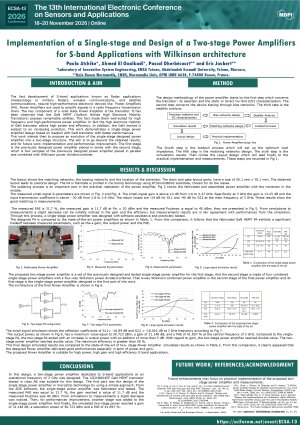
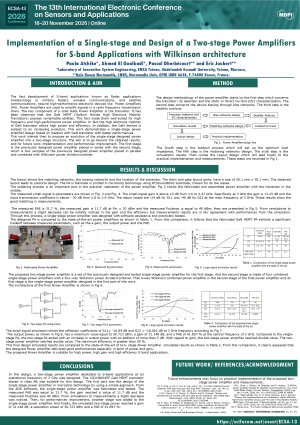
The contribution of this paper relies on the presentation of the design process, implementation, and practical measurements of a single-stage S-band power amplifier. This design will be extended into a two-stage power amplifier. The targeted S-band applications are wireless communications, satellite communications, and Radar systems. The selected transistor for this design is a GaN HEMT transistor suitable for 2 to 4 GHz operation in class AB. The biasing and matching networks of the power amplifier were based on microstrip technology, by using RT/duroid6002 substrate for loss reduction. The loadpull process and a simple matching network were used in this work. The simulated results of the power amplifier are at the central frequency of 3 GHz, a compression point at the input power of 28 dBm with a gain of 14.651 dB, a saturation power of 45.152 dBm, and a PAE (Power Added Efficiency) of 48.128 %. After measurements, the single-stage power amplifier demonstrated an output power of 40 dBm at the central frequency of 3 GHz, a maximum gain of 11.7 dB at Pin = 20 dBm and the PAE is 31.7 %. The simulated two-stage power reached a gain of 28.913 dB, a saturation power of 54.57 dBm and a PAE of 37.292 %. That last stage is made of eight combined single-stage power amplifiers with an eight-way Wilkinson power divider/combiner in order to increase the power. The obtained results demonstrate good features for S-band applications.
Keywords
Power amplifier
single-stage
S-band
two-stage
gain
efficiency
power.
Manuscript
Implementation of a Single-stage and Design of a Two-stage Power Amplifiers for S-band Applications with Wilkinson architecture- Pdf.pdf
Poster
Implementation of a Single-stage and Design of a Two-stage Power Amplifiers for S-band Applications with Wilkinson architecture- Pdf.pdf
Control of sensitivity and selectivity of piezoelectric sensor coatings and their application in assessing the content of petroleum products in sand
How Resolution Affects sEMG-Based Hand Gesture Recognition: A Machine Learning Preliminary Study