Event submissions
Published

This submission belongs to the session G. Posters of the event The 3rd International Electronic Conference on Materials
Published date
17 May, 2018
Citation
Randa Saad Hassan, Somaia Hassan Ali, Gamal Abdel Fattah, Studying the Effect of PbS Film Thickness on Morphology and Optical Properties, in Proceedings of The 3rd International Electronic Conference on Materials, 14 May–28 May 2018, MDPI: Basel, Switzerland, doi: 10.3390/ecms2018-05230
Share
Email
Facebook
Twitter
LinkedIn
Studying the Effect of PbS Film Thickness on Morphology and Optical Properties
'%3e%3cpath%20d='M12.6647%2010.9104C12.4176%2010.325%2012.0589%209.7933%2011.6088%209.34485C11.16%208.89511%2010.6283%208.53653%2010.0432%208.28891C10.038%208.28629%2010.0327%208.28498%2010.0275%208.28236C10.8437%207.69282%2011.3743%206.73252%2011.3743%205.64907C11.3743%203.85423%209.92005%202.40002%208.12522%202.40002C6.33038%202.40002%204.87618%203.85423%204.87618%205.64907C4.87618%206.73252%205.40677%207.69282%206.22296%208.28367C6.21772%208.28629%206.21248%208.2876%206.20724%208.29022C5.62031%208.53783%205.09365%208.89287%204.64167%209.34616C4.19192%209.79496%203.83334%2010.3266%203.58573%2010.9117C3.34247%2011.4846%203.21128%2012.0987%203.19925%2012.721C3.1989%2012.735%203.20135%2012.7489%203.20646%2012.7619C3.21157%2012.7749%203.21924%2012.7868%203.22901%2012.7968C3.23877%2012.8068%203.25045%2012.8148%203.26334%2012.8202C3.27623%2012.8256%203.29007%2012.8284%203.30406%2012.8284H4.09012C4.14776%2012.8284%204.19362%2012.7825%204.19493%2012.7262C4.22113%2011.7148%204.62726%2010.7676%205.34519%2010.0497C6.08802%209.30686%207.07452%208.89811%208.12522%208.89811C9.17592%208.89811%2010.1624%209.30686%2010.9052%2010.0497C11.6232%2010.7676%2012.0293%2011.7148%2012.0555%2012.7262C12.0568%2012.7839%2012.1027%2012.8284%2012.1603%2012.8284H12.9464C12.9604%2012.8284%2012.9742%2012.8256%2012.9871%2012.8202C13%2012.8148%2013.0117%2012.8068%2013.0214%2012.7968C13.0312%2012.7868%2013.0389%2012.7749%2013.044%2012.7619C13.0491%2012.7489%2013.0515%2012.735%2013.0512%2012.721C13.0381%2012.0947%2012.9084%2011.4856%2012.6647%2010.9104ZM8.12522%207.90243C7.52388%207.90243%206.95792%207.66793%206.53214%207.24215C6.10636%206.81636%205.87185%206.2504%205.87185%205.64907C5.87185%205.04773%206.10636%204.48177%206.53214%204.05599C6.95792%203.63021%207.52388%203.3957%208.12522%203.3957C8.72655%203.3957%209.29252%203.63021%209.7183%204.05599C10.1441%204.48177%2010.3786%205.04773%2010.3786%205.64907C10.3786%206.2504%2010.1441%206.81636%209.7183%207.24215C9.29252%207.66793%208.72655%207.90243%208.12522%207.90243Z'%20fill='%235D1EE1'/%3e%3c/g%3e%3c/svg%3e)
Randa Saad Hassan 1
Somaia Hassan Ali 1
Gamal Abdel Fattah 1
1. Department of laser sciences and interactions, National Institute of Laser Enhanced Sciences (NILES), Cairo University, Cairo, Egypt
Abstract
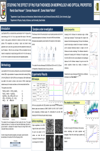
Lead Sulphide (PbS) is an important binary semiconductor from IV–VI group with a narrow band gap of 0.41 eV. It has a large exciton Bohr radius of 18nm which results in strong quantum confinement for electrons and holes even for large particles. PbS nanoparticles are promising in optical and photonic device applications such as solar cells, gas sensors and other optoelectronic devices and also IR detectors . When the size and shape of PbS are transferred from bulk material to nanoparticles, the optical band gap shifts from 0.41 eV to the values up to 5.2 eV which is suitable to build optical sensors with adjustable properties
In this work, PbS thin films were deposited on glass substrates by chemical bath deposition method. We observe that the film thickness was doubled by repeating the chemical reaction. The effect of varying film thickness on structure and optical properties was studied. XRD reveals that all of the films were polycrystalline with (200) preferred crystal orientation. Increasing the film thickness enhances the crystallinity as well as reduces the dislocation density and strain of the films. Optical measurements show that as the thickness of the PbS film increases, the band gap of the films decreases from 1.47eV to 0.77eV and shifts from visible region to IR region. One of the prepared samples was used as an IR detector in the range of (800 nm to 1800 nm) it shows good agreement with the commercial PbS detector .
Keywords
PbS thin films
energy gap
thickness effect
optical properties
IR detector
Poster
Dr. Randa 's POSTER1.pdf
Study of the Properties of Co-Substituted Ba2Mg2Fe12O22 Hexaferrites
Effects of Silica Fume on the Pore Structure and Properties of Mortars Exposed to Sulphate Aggressive Media